
We have observed over the years that technology has changed continuously and been able to squeeze itself in a more compact and concise structure. Let’s take an illustration of this the principal computers which are made were the length of a warehouse of 1000 laptops which we use today. Consider how this has been made possible? The answer to it’s integrated circuits.
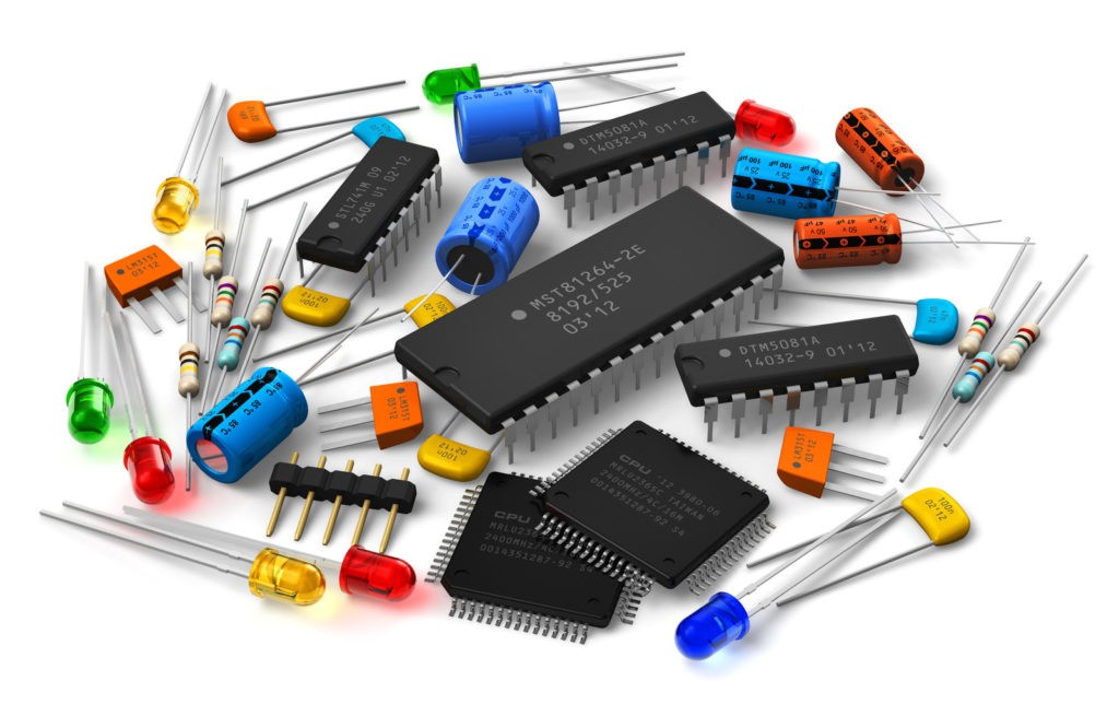
The circuits that were made previously were very large and hulking, because of its circuit components like resistor, transistor, diodes, capacitor, inductor, etc. which are connected alongside copper wires. This factor limited the utilization of the circuits to big machines. It was impossible to produce smaller than average compact appliances with one of these big circuits. Moreover, they weren’t entirely shockproofed and reliable.
As mentioned, necessity is the mother of all inventions, similarly, the latest technologies all are the effect of it. There was clearly absolutely vital to formulate circuits of smaller size with more power and safety to incorporate them into devices. Then were three American scientists who invented transistors which simplified what to quite an extent, but it was the roll-out of integrated circuits that changed the face of electronics technology.
Precisely what is Integrated Circuit?
A built-in circuit (IC), it often may be known as a chip or possibly a microchip is often a series of transistors which are put on silicon. A circuit is way too small in size, if it is when compared to the standard circuits that are made of the independent circuit components, it’s about the size of a fingernail. IC is really a semiconductor wafer (also referred to as a skinny slice of semiconductor, for example crystalline silicon) where thousands or countless tiny resistors, capacitors, and transistors are fabricated.
Modern electronic circuits aren’t comprised of individual, ensures they can not be composed of separated components as used to be true. Instead, many small circuits take root within a complex part of silicon and also other materials called an internal circuit(IC), or chip or microchip. The manufacture of integrated circuits commences with a simple circular wafer of silicon several inches across.
Firstly designers made drawings of where by each aspect in each part of the circuit is to go so the processing would become easy. A photo of each diagram will be reduced in space repeatedly to produce a tiny photolithographic mask.
The silicon wafer is coated with a material known as a photoresist that undergoes a compound process when encountered with ultraviolet light. Ultraviolet light shown over the mask on top of the photoresist creates an equivalent pattern on the wafer as just like that mask. Then solvents etch into the elements of the resist that have been exposed to the sunshine, leaving the opposite parts intact. Then another layer of a silicon material doped with many impurities so that it’s laid down into the wafer, and the other pattern is etched in by the similar technique.
The effect of these operations is a multilayered circuit, with lots of numerous tiny transistors, resistors, and conductors created within the wafer. The wafer will be broken apart along prestressed lines into many identical square or rectangular chips, that’s no more integrated circuits.
To read more about ALL NEW SEMI go the best net page